그래핀 샘플
제품 소개
CVD(화학기상증착법)으로 합성된 고품질의 그래핀입니다.
95% 이상의 단일층 그래핀으로 구성되어 있습니다.
저희 그래핀스퀘어는 그래핀 연구와 최신 기술의 응용연구를 하시는
그래핀 연구자를 위해 다양한 연구와 측정 자료를 제공하고 있습니다.
95% 이상의 단일층 그래핀으로 구성되어 있습니다.
저희 그래핀스퀘어는 그래핀 연구와 최신 기술의 응용연구를 하시는
그래핀 연구자를 위해 다양한 연구와 측정 자료를 제공하고 있습니다.
Size
50 mm x 50 mm, 1ea
2″ x 2″, 1ea
80 mm x 80 mm, 1ea
3″ x 3″, 1ea
2″ x 2″, 1ea
80 mm x 80 mm, 1ea
3″ x 3″, 1ea
Properties of Graphene
Product Size : Up to 500x600 ㎟
Film morphology : Continuous Monolayer(>95%)
Sheet Resistance : Av. < 250~400 Ω/sq (after transfer)
Mobility : >3500 ㎠/Vs
Transmittance : >97%
Domain Size : ~10 ㎛
Film morphology : Continuous Monolayer(>95%)
Sheet Resistance : Av. < 250~400 Ω/sq (after transfer)
Mobility : >3500 ㎠/Vs
Transmittance : >97%
Domain Size : ~10 ㎛
Properties of Substrate
Material : Copper
Purity : ~99.9%
Type : flexible foil
Thickness : ~35㎛
Purity : ~99.9%
Type : flexible foil
Thickness : ~35㎛
Applications
Transparent electrode (flexible display & touch screen)
Energy electrode (solar cells, secondary batteries, fuel cells, supercapacitors)
Functional composite materials (ultra-light strong composite for cars & aerospace)
Heat dissipation (LED lighting & ECU units)
Barrier (gas barriers, electromagnetic wave barriers)
Biomedical applications (substrate for stem cell therapy, graphene liquid cells for electron microscopy)
Main Target
Those who want to proceed directly to a Graphene transfer process
Measurement Data
그래핀스퀘어의 CVD그래핀은 균일하고 뛰어난 품질을 보여줍니다.
*Raman spectroscope measurement conditions
Laser : 514 nm / Laser Power : 100% / Exposure time : 10s / Accumulation number : 1 /
Hole size : 1 um / Grating : 1200
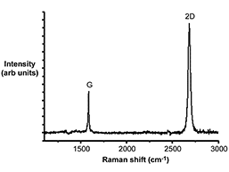
Raman Spectrum (after transfer)
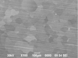
High Revolution SEM Image
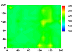
Sheet Resistance Uniformity
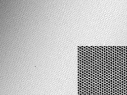
High Revolution TEM Image
Reference
S. Bae*, H. Kim* et al.Roll-to-roll production of 30 inch graphene films for transparent electrodes Nature Nanotech.5, 574 (2010).
Y. Lee et al. Wafer-Scale Synthesis and Transfer of Graphene Films. Nano Lett. 10, 490-493 (2010).
H.-A-S. Shin et al. Graphene-induced Unusual Microstructural Evolution in Ag Plated Cu Foils. Nanoscale 6, 7209-7214 (2014).
Hae-A-Seul Shin*, Jaychul Ryu* et al. Highly Uniform Growth of Monolayer Graphene by Chemical Vapor Deposition on Cu-Ag Alloy Catalysts. Phys. Chem. Chem. Phys. 16, 3087-3094 (2014).
Package

타사와 달리 연구에 사용할 그래핀 표면에 접촉이 없어 물리적인 긁힘(scratch)으로부터 안전합니다.
그래핀 핸들링이 쉽도록 샘플 하부에 PET film을 지지층으로 사용하였습니다.
간단히 PET를 케이스에서 떼어내어 사용하십시오.
보관 방법
Oxygen에 의한 영향을 줄이기 위해서 발송되는 진공포장 상태를 유지하거나,
개봉 후에는 진공 데시케이터에서 보관하십시오.
구매 고객 리스트
| ETH Zurich | University of Exeter |
| Nokia Research Center | Sabanci University |
| Seoul National University | Korea Atomic Energy Research Institute |
| Intel Corporation | University of Oxford |
| Edicogenome | Korea Advanced Institute of Science and Technology |
| Ulsan National Institute of Science and Technology | Korea Basic Science Institute |
| University of Applied Sciences, Berlin | University of Westminster |
| Korea Institute of Science and Technology | Korea Institute of Ceramic |
| Korea University | Korea Aerospace University |
그래핀스퀘어의 특장점
세계최초! 대면적 그래핀을 합성한 그래핀 스퀘어

Nature Nanotechnology 2010 cover image.
다년간의 Transfer 노하우

최적화된 연구 환경에서 진행됩니다. Less residue, clear surface, Coverage 95% 이상,
기판 표면 개질 등
그래핀 손상을 최소화하는 Package

질소 충진 진공포장 표면 contact zero Handling이 용이한 packing
Optimized Graphene

옵션/추가공정으로 연구방향에 맞는 그래핀 샘플 advice 그래핀 연구 경험이 없으신 분들, 새로운 기판에 그래핀 적용을 원하시는 분들께 추천합니다.
확실한 Warranty Service

품질 이상 시, 100% 재제작 언제든 연락주세요.
CVD 합성 그래핀부터 장비 판매까지
All about Graphene

장비부터 Transfer까지 모든 공정에 대한 이해를 기반으로 오직 그래핀만을 위한 CVD 장비 취급부터 그래핀만을 위한 합성, 전사, 포장 공정.
배송
포장 과정
01
질소 충전, 진공 포장

02
완충재 포장
03
택배사 픽업
| 주문 과정 |

고객 주문/결제 |

그래핀 샘플 제작 |

포장 |

배송(우체국 택배 이용) |
|---|---|---|---|---|
| 진행 현황 |
고객의 주문을
확인하고 검토합니다 |
고품질 샘플을 제작하고
품질검사를 진행합니다 |
운반과 취급에 대비해
안전하게 포장합니다 |
주문하신 제품을 발송합니다
(일반적으로 3영업일이 소요됩니다) |
문의
샘플 및 장비 관련 문의는
info@graphenesq.com
으로 부탁드립니다.