Graphene Samples
CVD Graphene on Glass
This product consists of graphene transferred onto a quartz plate using a PMMA (Poly(methyl methacrylate)) support layer.
※Large-Area Graphene Available for Purchase
Product and Service Overview
The state of the art chemical vapor deposition (CVD) method is used to synthesize our high-quality graphene products. It boasts more than 90% coverage of mono-layer graphene.
We also provide various studies and measurements on graphene samples to meet your need for high-end research and application.
Size
10 mm x 10 mm, 4ea
10 mm X 10 mm, 10ea
10 mm X 10 mm, 20ea
50 mm X 50 mm, 1ea
2″ x 2″, 1ea
3″ x 3″, 1ea
80 mm X 80 mm, 1ea
10 mm X 10 mm, 10ea
10 mm X 10 mm, 20ea
50 mm X 50 mm, 1ea
2″ x 2″, 1ea
3″ x 3″, 1ea
80 mm X 80 mm, 1ea
Properties of Graphene
Product Size : Up to 140x140 ㎟(8" wafer)
Film morphology : Continuous Monolayer(>95%)
Sheet Resistance : Av. < 250~400 Ω/sq (after transfer)
Mobility : >3500 ㎠/Vs (Max. 17.000 ㎠/Vs)
Transmittance : >97%
Subtrate : Quartz plate (1T) (Standard)
Domain Size:~10 ㎛
Film morphology : Continuous Monolayer(>95%)
Sheet Resistance : Av. < 250~400 Ω/sq (after transfer)
Mobility : >3500 ㎠/Vs (Max. 17.000 ㎠/Vs)
Transmittance : >97%
Subtrate : Quartz plate (1T) (Standard)
Domain Size:~10 ㎛
Specifications
Flame fused ingots are re-heated to make many shaped plates. This plates can be used for window material, mask substrate and flanges.
Another hand the ingot is drawn to rod for quartz boat, fabrication welding rod and optical fiber parts. OH contents will be 120~260 ppm as general
Chemical element composition (Typical data)
| Al | Fe | K | Li | Cu | NaS | B | Ca | Mg | P | Ti | OH |
| 20.00 | 0.40 | 1.00 | 1.4 | 0.01 | 1.50 | 0.20 | 0.50 | - | - | - | - |
Transparent Quartz Glass Property
| Density | 2.21 × 10³ kg/m³ |
| Hardness | 580 KHN100 |
| Tensile Strength | 4.9 × 10⁷ Pa (N/m²) |
| Compression Strength | > 1.1 × 10⁹ Pa |
| Coefficient of Thermal Expansion (20–300℃) | 5.5 × 10⁻⁷ cm/cm·℃ |
| Thermal Conductivity (20℃) | 1.4 W/m·℃ |
| SpecificHeat (20℃) | 680 J/kg·℃ |
| Softening Point | 1700℃ |
| Annealing Point | 1210℃ |
Optical property
Our transparent quartz material has excellent transmission, especially ultra-red zone and visible area compare with ordinary glass.
Transmission of UV is related with metal impurities. 2730nm wave indicate OH content absorption and volume.
Applications
Transparent electrode (flexible display & touch screen)
Energy electrode (solar cells, secondary batteries, fuel cells, supercapacitors)
Functional composite materials (ultra-light strong composite for cars & aerospace)
Heat dissipation (LED lighting & ECU units)
Barrier (gas barriers, electromagnetic wave barriers)
Biomedical applications (substrate for stem cell therapy, graphene liquid cells for electron microscopy)
Main Target
For those researchers who do not have much experience in Graphene transfer process
For those researchers in need of graphene transfer onto transparent and flexible circuit board
For those researchers in need of high quality Graphene on Quartz glass
For those researchers in need of graphene transfer onto transparent and flexible circuit board
For those researchers in need of high quality Graphene on Quartz glass
Additional Options
Reduce sheet resistance by BI doping.
Reduce sheet resistance by Multi-layers graphene (Graphene stacking, laminated). (ex. 2, 3, 4, …, 10-layers)
Various sizes.
Transfer graphene onto Electrode patterned boards.
Reduce sheet resistance by Multi-layers graphene (Graphene stacking, laminated). (ex. 2, 3, 4, …, 10-layers)
Various sizes.
Transfer graphene onto Electrode patterned boards.
Measurement Data
Graphene Square’s CVD graphene demonstrates uniformity and outstanding quality.
*Raman spectroscope measurement conditions
Laser : 514 nm / Laser Power : 100% / Exposure time : 10s / Accumulation number : 1 /
Hole size : 1 um / Grating : 1200
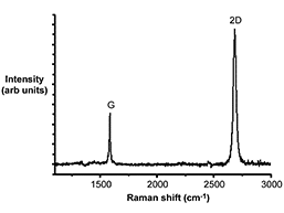
Raman Spectrum (after transfer)
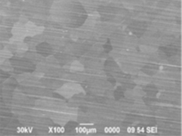
High Revolution SEM Image
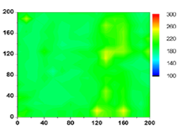
Sheet Resistance Uniformity
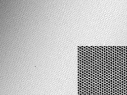
High Revolution TEM Image
Reference
S. Bae*, H. Kim* et al. Roll-to-roll production of 30 inch graphene films for transparent electrodes Nature Nanotech. 5, 574 (2010).
Y. Lee et al. Wafer-Scale Synthesis and Transfer of Graphene Films. Nano Lett. 10, 490-493 (2010).
S. J. Kim*, T. Choi* et al. "Ultra-Clean Patterned Transfer of Single-Layer Graphene by Recyclable Pressure Sensitive Adhesive Films" Nano Letters 15, 3236?3240 (2015).
Y. Lee et al. Wafer-Scale Synthesis and Transfer of Graphene Films. Nano Lett. 10, 490-493 (2010).
S. J. Kim*, T. Choi* et al. "Ultra-Clean Patterned Transfer of Single-Layer Graphene by Recyclable Pressure Sensitive Adhesive Films" Nano Letters 15, 3236?3240 (2015).
Package

We have taken special care and use vacuum packaging to minimize damage on the research surface of graphene. Our graphene film sample packaging is unique such that the graphene surface does not come in contact with the inner package surface. As a result, our graphene samples are not damaged nor scratched during the shipping process. We suggest use of tweezers to handle graphene.
Storage Instructions
To minimize the effects of oxygen, keep the graphene in its vacuum-sealed packaging during shipment, or store it in a vacuum desiccator after opening.
Customer List
| National University of Singapore | Sabanci University |
| Nokia Research Center | Korea Basic Science Institute |
| HRL Laboratories | Seoul National University |
| LG Display | SungKyunKwan University |
| Korea Advanced Institute of Science and Technology | University of Bari Aldo Moro |
| Korea Atomic Energy Research Institute | Agency for Defense Development |
Graphene Square Advantages
World’s first large scale graphene synthesis towards commercialization.

Nature Nanotechnology 2010 cover image.
Many years of know-how in transfer method.

Coverage at above 95%, low residue. Most optimized R&D environment.
Our sample package is designed to minimize graphene damage.

Vacuum packaged, nitrogen filled. Easy to handle.
Optimized Graphene

We give advice and make suggestions to the beginners in graphene research. Offer Graphene on various and unique substrates.
Our commitment

We promise to deliver a level of quality unmatched and to our customers’ satisfaction.
All about Graphene-from thermal CVD equipment to graphene synthesis and transfer process with know-how.

Understanding of the whole process from the graphene synthesis, transfer, proper packaging with sound research is our key to success.
Delivery
Packaging Process
01
Vacuum packaging, nitrogen filled
02
Air cushion packaging
03
Ready for pick up by courier service
| Order process |

Customer order and |

Produce graphene |

Packaging |

Delivery |
|---|---|---|---|---|
| Status |
Review and confirm
customer order |
Produce and inspect for
high quality product |
Expert and protective
packaging for S&H |
Estimated time of delivery is three business days
(Detailed shipment tracking on fedex.com) |
Inquiry
Please email to info@graphenesq.com for sample/equipment inquiries