Graphene Samples
Graphene on Cu foil
This product features graphene synthesized on both sides of a copper foil. Please use the visible top side.
※Large-Area Graphene Available for Purchase
Product and Service Overview
The state of the art chemical vapor deposition (CVD) method is used to synthesize our high-quality graphene products. It boasts more than 90% coverage of mono-layer graphene.
We also provide various studies and measurements on graphene samples to meet your need for high-end research and application.
Size
50 mm x 50 mm, 1ea
2″ x 2″, 1ea
80 mm x 80 mm, 1ea
3″ x 3″, 1ea
2″ x 2″, 1ea
80 mm x 80 mm, 1ea
3″ x 3″, 1ea
Properties of Graphene
Product Size : Up to 500x600 ㎟
Film morphology : Continuous Monolayer(>95%)
Sheet Resistance : Av. < 250~400 Ω/sq (after transfer)
Mobility : >3500 ㎠/Vs
Transmittance : >97%
Domain Size : ~10 ㎛
Film morphology : Continuous Monolayer(>95%)
Sheet Resistance : Av. < 250~400 Ω/sq (after transfer)
Mobility : >3500 ㎠/Vs
Transmittance : >97%
Domain Size : ~10 ㎛
Properties of Substrate
Material : Copper
Purity : ~99.9%
Type : flexible foil
Thickness : ~35㎛
Purity : ~99.9%
Type : flexible foil
Thickness : ~35㎛
Applications
Transparent electrode (flexible display & touch screen)
Energy electrode (solar cells, secondary batteries, fuel cells, supercapacitors)
Functional composite materials (ultra-light strong composite for cars & aerospace)
Heat dissipation (LED lighting & ECU units)
Barrier (gas barriers, electromagnetic wave barriers)
Biomedical applications (substrate for stem cell therapy, graphene liquid cells for electron microscopy)
Main Target
Those who want to proceed directly to a Graphene transfer process
Measurement Data
Graphene Square’s CVD graphene demonstrates uniformity and outstanding quality.
*Raman spectroscope measurement conditions
Laser : 514 nm / Laser Power : 100% / Exposure time : 10s / Accumulation number : 1 /
Hole size : 1 um / Grating : 1200
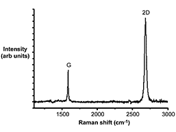
Raman Spectrum (after transfer)
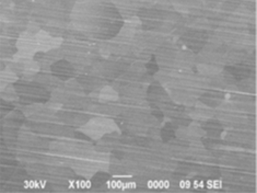
High Revolution SEM Image
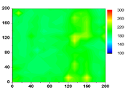
Sheet Resistance Uniformity
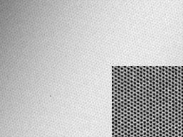
High Revolution TEM Image
Reference
S. Bae*, H. Kim* et al.Roll-to-roll production of 30 inch graphene films for transparent electrodes Nature Nanotech.5, 574 (2010).
Y. Lee et al. Wafer-Scale Synthesis and Transfer of Graphene Films. Nano Lett. 10, 490-493 (2010).
H.-A-S. Shin et al. Graphene-induced Unusual Microstructural Evolution in Ag Plated Cu Foils. Nanoscale 6, 7209-7214 (2014).
Hae-A-Seul Shin*, Jaychul Ryu* et al. Highly Uniform Growth of Monolayer Graphene by Chemical Vapor Deposition on Cu-Ag Alloy Catalysts. Phys. Chem. Chem. Phys. 16, 3087-3094 (2014).
Package

We have taken special care and use vacuum packaging to minimize damage on the research surface of graphene. Our graphene film sample packaging is unique such that the graphene surface does not come in contact with the inner package surface. As a result, our graphene samples are not damaged nor scratched during the shipping process. In addition, we used PET film on the bottom side for protection.
Storage Instructions
To minimize the effects of oxygen, keep the graphene in its vacuum-sealed packaging during shipment, or store it in a vacuum desiccator after opening.
Customer List
| ETH Zurich | University of Exeter |
| Nokia Research Center | Sabanci University |
| Seoul National University | Korea Atomic Energy Research Institute |
| Intel Corporation | University of Oxford |
| Edicogenome | Korea Advanced Institute of Science and Technology |
| Ulsan National Institute of Science and Technology | Korea Basic Science Institute |
| University of Applied Sciences, Berlin | University of Westminster |
| Korea Institute of Science and Technology | Korea Institute of Ceramic |
| Korea University | Korea Aerospace University |
Graphene Square Advantages
World’s first large scale graphene synthesis towards commercialization.

Nature Nanotechnology 2010 cover image.
Many years of know-how in transfer method.

Coverage at above 95%, low residue. Most optimized R&D environment.
Our sample package is designed to minimize graphene damage.

Vacuum packaged, nitrogen filled. Easy to handle.
Optimized Graphene

We give advice and make suggestions to the beginners in graphene research. Offer Graphene on various and unique substrates.
Our commitment

We promise to deliver a level of quality unmatched and to our customers’ satisfaction.
All about Graphene-from thermal CVD equipment to graphene synthesis and transfer process with know-how.

Understanding of the whole process from the graphene synthesis, transfer, proper packaging with sound research is our key to success.
Delivery
Packaging Process
01
Vacuum packaging, nitrogen filled
02
Air cushion packaging
03
Ready for pick up by courier service
| Order process |

Customer order and |

Produce graphene |

Packaging |

Delivery |
|---|---|---|---|---|
| Status |
Review and confirm
customer order |
Produce and inspect for
high quality product |
Expert and protective
packaging for S&H |
Estimated time of delivery is three business days
(Detailed shipment tracking on fedex.com) |
Inquiry
Please email to info@graphenesq.com for sample/equipment inquiries