Graphene Samples
CVD Graphene on TEM Grid
For Transmission Electron Microscope (TEM) measurements, we transfer monolayer TCVD graphene on Cu foil onto a TEM grid.
If you prefer 0% PMMA, please leave a note specifying your request.
If you prefer 0% PMMA, please leave a note specifying your request.
※Large-Area Graphene Available for Purchase
Product and Service Overview
The state of the art chemical vapor deposition (CVD) method is used to synthesize our high-quality graphene products. It boasts more than 90% coverage of mono-layer graphene.
We also provide various studies and measurements on graphene samples to meet your need for high-end research and application.
Properties of Graphene
Grid Hole Size : 63 μm
Sheet Resistance : Av.< 250~400 Ω/sq
Lacey Carbon Type-A
Mobility : >3500 ㎠/Vs (Max. 17,000 ㎠/Vs
300 mesh
Transmittance : >97%
Copper Frame
Coverage : <30% (PMMA-free), <60% (2-layers)
Sheet Resistance : Av.< 250~400 Ω/sq
Lacey Carbon Type-A
Mobility : >3500 ㎠/Vs (Max. 17,000 ㎠/Vs
300 mesh
Transmittance : >97%
Copper Frame
Coverage : <30% (PMMA-free), <60% (2-layers)
Specifications
Lacey Carbon Type-A
A Lacey carbon film with a removable Formvar backing on the opposite side of the grid. When the Formvar is removed, by dipping in solvent, the Lacey carbon film remains. These films are stable under all EM(electron microscopy) operating conditions and for use where the presence of Formvar can not be tolerated. Pure Lacey Carbon is more delicate than those with Formvar backing and require more careful handling during specimen preparation. Holes are completely open.

Support Film Product Note, How the Material is Layered on the Grid
Most of the grids used have a distinct “shiny” side and “dull” side when viewed with the naked eye. Generally, the film type as specified in the product name lies on the shiny side of the grid.
Lacey carbon Type A
The Lacey formvar film is applied to the dull side of the grid and carbon depositied onto the shiny side. When the formvar is removed in solvent the carbon film is left on the shiny side.
Grid Cross Section

Substrate Application |
Carbon Type-A |
Is Lacey Film suitable for this application? |
Applications Requiring Pure Formvar |
Not Suitable |
No |
Bacterial Suspensions |
Best |
Yes |
Cell Fragment Suspensions |
Best |
Yes |
Diffraction Studies |
Best |
Yes |
EDS (energy dispersive spectrometry) |
Best |
Yes |
High Resolution Microscopy |
Best |
Yes |
High Temperature Techniques / Heating Stage |
Best |
Yes(Type-A) |
Low Magnification Microscopy |
Good Alternative |
No |
Particulate Suspension, Biological |
Best |
Yes |
Particulate Suspension, Non-Biological |
Best |
Yes |
Powders, Dry |
Good Alternative |
No |
Replicas & Low Temperature Techniques |
Good Alternative |
Yes(Type-A) |
Thin Sections |
Good Alternative |
Yes |
Viral Suspensions | Best | Yes |
Measurement data

(d) HR-TEM results showing the atomic lattice structures of RT-CVD graphene. The graphene samples were prepared with holey carbon grid (upper inset). The aberration-corrected scanning TEM image provides an atom-by-atom analysis of graphene (mid inset). The diffraction pattern indicates the corresponding graphene is a highly crystalline monolayer (lower inset).
(e) Graphene domain distribution investigated by selected area diffraction patterns (SADP) and TEM imaging. (f) Graphene boundaries of RT-CVD graphene characterized by dark-field TEM and aberration-corrected HR-TEM images . The left and right parts of the grain boundary are imaged with an aperture at the red and blue circled spots of the diffraction pattern (upper inset). The atomic image shows that two graphene domains are smoothly connected with an angle of 36° (lower inset). See also Supporting Figure S2 for more dark-field TEM analyses.

Figure 4. Grain boundary analyses by TEM and OM. (a-c) Grain boundary mapping of RT-CVD graphene films by TEM corresponding to the sheet resistance of spots 1, 2, and 3 in Figure 3a, respectively. (d-f) Grain boundary mapping of H2O2-treated RT-CVD graphene on Cu foils by optical microscopes, corresponding to the red spots 1, 2, and 3 in Figure 3a, respectively. The grain size of graphene in the center region is a few times larger than the edge region. But actually, there is no significant difference in sheet resistance (226, 227, and 230 Ω/sq for spots 1, 2, and 3, respectively).

Figure 1 | Morphology of nanobubbles in graphene liquid cell. (a?d) A graphene liquid cell fabricated on a ?at TEM grid (copper or molybdenum) showing the top views of nanobubbles. (c and d) In-situ snapshot images of nanobubbles obtained by ultra-high vacuum (UHV) TEM (200 keV, ~5X10⁻⁹ Torr). Scale bars, 10 nm. (e?g) A folded graphene liquid cell showing the side views of nanobubbles. The contact angles were roughly measured to be 6o°?90°. Scale bars for f and g, 10 and 5 nm, respectively.

Figure 2 l Time evolution of different kinds of single and double nanobubbles. (a,b) The snap shots of Tem images showing the vanishing and stable nanobubbles, respectively. The nanobubbles smaller than critical radius tend to shrink with time and disappear in ~40s, whereas the larger bubbles persist for more than 10 min. Scale bar, 5 nm. The full movie is available in Supplementary Movie 2. (c,d) The snap shots of TEM images showing the merging of adjacent two nanobubbles observed for 15 and 50 s, respectively. When the nanobubble sizes are significantly different, it show an Ostwald ripening-like merging process, whereas the similar-sized bubbles are coalescing as their inter-bubble boundary breaks. Scale bar, 10nm. The full movie is available in Supplementary Movie 3.
Measurement Data
Graphene Square’s CVD graphene demonstrates uniformity and outstanding quality.
*Raman spectroscope measurement conditions
Laser : 514 nm / Laser Power : 100% / Exposure time : 10s / Accumulation number : 1 /
Hole size : 1 um / Grating : 1200
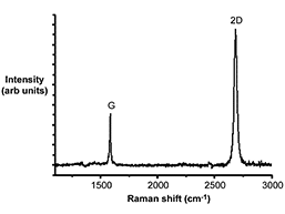
Raman Spectrum (after transfer)
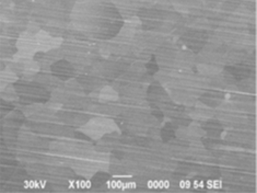
High Revolution SEM Image
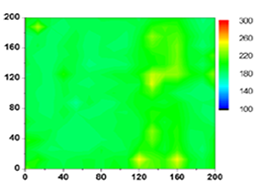
Sheet Resistance Uniformity
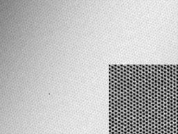
High Revolution TEM Image
Reference
Ryu, Jaechul, et al. "Fast synthesis of high-performance graphene films by hydrogen-free rapid thermal chemical vapor deposition.” ACS nano 8.1 (2014): 950-956.
Park, Jooyeon, et al. “Graphene?Regulated Cardiomyogenic Differentiation Process of Mesenchymal Stem Cells by Enhancing the Expression of Extracellular Matrix Proteins and Cell Signaling Molecules.” Advanced healthcare materials 3.2 (2014): 176-181.
Shin, Dongha, et al. “Growth dynamics and gas transport mechanism of nanobubbles in graphene liquid cells." Nature communications 6 (2015).
Kim, Yeonho, et al. "High-performance ultraviolet photodetectors based on solution-grown ZnS nanobelts sandwiched between graphene layers." Scientific reports 5 (2015).
Sim, Uk, et al. "N-doped graphene quantum sheets on silicon nanowire photocathodes for hydrogen production." Energy & Environmental Science 8.4 (2015): 1329-1338.
Moon, Joonhee, et al. "One?Step Synthesis of N?doped Graphene Quantum Sheets from Monolayer Graphene by Nitrogen Plasma." Advanced Materials 26.21 (2014): 3501-3505.
Kim, Sang Jin, et al. "Simultaneous etching and doping by Cu-stabilizing agent for high-performance graphene-based transparent electrodes." Chemistry of Materials 26.7 (2014): 2332-2336.
Kim, Jung Kyu, et al. "Surface-Engineered Graphene Quantum Dots Incorporated into Polymer Layers for High Performance Organic Photovoltaics." Scientific reports 5 (2015).
Storage Instructions
To minimize the effects of oxygen, keep the graphene in its vacuum-sealed packaging during shipment, or store it in a vacuum desiccator after opening.
Graphene Square Advantages
World’s first large scale graphene synthesis towards commercialization.

Nature Nanotechnology 2010 cover image.
Many years of know-how in transfer method.

Coverage at above 95%, low residue. Most optimized R&D environment.
Our sample package is designed to minimize graphene damage.

Vacuum packaged, nitrogen filled. Easy to handle.
Optimized Graphene

We give advice and make suggestions to the beginners in graphene research. Offer Graphene on various and unique substrates.
Our commitment

We promise to deliver a level of quality unmatched and to our customers’ satisfaction.
All about Graphene-from thermal CVD equipment to graphene synthesis and transfer process with know-how.

Understanding of the whole process from the graphene synthesis, transfer, proper packaging with sound research is our key to success.
Delivery
Packaging Process
01
Vacuum packaging, nitrogen filled
02
Air cushion packaging
03
Ready for pick up by courier service
| Order process |

Customer order and |

Produce graphene |

Packaging |

Delivery |
|---|---|---|---|---|
| Status |
Review and confirm
customer order |
Produce and inspect for
high quality product |
Expert and protective
packaging for S&H |
Estimated time of delivery is three business days
(Detailed shipment tracking on fedex.com) |
Inquiry
Please email to info@graphenesq.com for sample/equipment inquiries